Go to
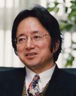
Shunri Oda
Nanoelectronic Circuits and Tools
14-18 July 2008, EPFL Auditorium CO3
 Professor
Department of Physical Electronics
Quantum Nanoelectronics Research Center
Tokyo Institute of Technology, Tokyo, Japan
Webpage
Lecture 1: Tuesday, 15 July 2008 (10h00-11h00) CO3
Silicon quantum dots: the future of electronics and photonics?
Quantum dot structures, where electrons are confined three-dimensionally in the sub-10 nm scale, show characteristics quite different from conventional bulk structures. Recent progress in the fabrication technology of silicon nanostructures has made possible observations of novel electrical and optical properties of silicon quantum dots, such as single electron tunneling, ballistic transport, visible photoluminescence and electron emission. Electron transport and photonic properties of silicon nanocrystals prepared by plasma processes will be presented with particular emphasis on the fabrication of monodispersed silicon nanocrystals, high-density assembly of silicon quantum dots. I will also discuss applications of silicon quantum dots to nanodot memory for future Tera bit non-volatile memory devices, and silicon photonic devices for future ULSI interconnections.
Lecture 2: Tuesday, 15 July 2008 (11h15-12h15) CO3
Novel Nano-ElectroMechanical-System Devices
A nanoelectromechanical device incorporating the nanocrystalline silicon (nc-Si) dots is proposed for use as a high-speed and nonvolatile memory. The nc-Si dots are embedded as charge storage in a mechanically bistable floating gate. Position of the floating gate can therefore be switched between two stable states by applying gate bias and its flip-flop motion can be sensed electrically by MOSFET underneath. Superior on-off characteristics are demonstrated by using an equivalent circuit model which takes account of the variable capacitance due to the mechanical displacement of the floating gate. Mechanical property analysis conducted by using the finite element method shows that introduction of nc-Si dot array into the movable floating gate results in reduction of switching power. High switching frequency over 1 GHz is achieved by decreasing the length of the floating gate to the submicron regime. I also present experimental demonstration of the mechanical bistability of the SiO2 beams fabricated by using the conventional silicon etching processes.
About the speaker:
Shunri Oda received the B. Sc degree in physics, the M. Eng. and Dr. Eng. degree from Tokyo Institute of Technology in 1974, 1976 and 1979, respectively. He is a Professor in Department of Physical Electronics and Quantum Nanoelectronics Research Center, Tokyo Institute of Technology. His current research interests include fabrication of silicon quantum dots by pulsed plasma processes, single electron tunneling devices based on nanocrystalline silicon, ballistic transport in silicon nanodevices, silicon based photonic devices, and high-k gate oxide ultrathin films prepared by atomic layer MOCVD. He has authored approximately 200 international technical and more than 230 conference papers including more than 70 invited papers. He edited a book (with D. Ferry) "Silicon Nanoelectronics" (CRC Press, 2006).
Prof. Oda is a member of Electrochemical Society, Materials Research Society, and a Fellow of Japan Society for Applied Physics. He is a Distinguished Lecturer of IEEE Electron Devices Society.
Secondary navigation
- EPFL Workshop on Logic Synthesis and Emerging Technologies
- Luca Amaru
- Luca Benini
- Giovanni De Micheli
- Srini Devadas
- Antun Domic
- Rolf Drechsler
- Pierre-Emmanuel Gaillardon
- Jie-Hong Roland Jiang
- Akash Kumar
- Shahar Kvatinsky
- Yusuf Leblebici
- Shin-ichi Minato
- Alan Mishchenko
- Vijaykrishnan Narayanan
- Ian O'Connor
- Andre Inacio Reis
- Martin Roetteler
- Julien Ryckaert
- Mathias Soeken
- Christof Teuscher
- Zhiru Zhang
- Symposium on Emerging Trends in Computing
- Layout synthesis: A golden DA topic
- EPFL Workshop on Logic Synthesis & Verification
- Luca Amaru
- Luca Benini
- Robert Brayton
- Maciej Ciesielski
- Valentina Ciriani
- Jovanka Ciric-Vujkovic
- Jason Cong
- Jordi Cortadella
- Giovanni De Micheli
- Antun Domic
- Rolf Drechsler
- Henri Fraisse
- Paolo Ienne
- Viktor Kuncak
- Enrico Macii
- Igor Markov
- Steven M. Nowick
- Tsutomu Sasao
- Alena Simalatsar
- Leon Stok
- Dirk Stroobandt
- Tiziano Villa
- Symposium on Emerging Trends in Electronics
- Raul Camposano
- Anantha Chandrakasan
- Jo De Boeck
- Gerhard Fettweis
- Steve Furber
- Philippe Magarshack
- Takayasu Sakurai
- Alberto Sangiovanni-Vincentelli
- Ken Shepard
- VENUE
- Panel on Circuits in Emerging Nanotechnologies
- Panel on Emerging Methods of Computing
- Panel on The Role of Universities in the Emerging ICT World
- Panel on Design Challenges Ahead
- Panel on Alternative Use of Silicon
- Nano-Bio Technologies for Lab-on-Chip
- Functionality-Enhanced Devices Workshop
- More Moore: Designing Ultra-Complex System-on-Chips
- Design Technologies for a New Era
- Nanotechnology for Health
- Secure Systems Design
- Surface Treatments and Biochip Sensors
- Security/Privacy of IMDs
- Nanosystem Design and Variability
- Past Events Archive

