Go to
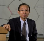
Philip Wong
Nanoelectronic Circuits and Tools
14-18 July 2008, EPFL Auditorium CO3
Department of Electrical Engineering
Center for Integrated Systems
Stanford University, Stanford, CA - USA
Webpage
Lecture 1: Monday, 14 July 2008 (10h00-11h00) CO3
Beyond CMOS Scaling - What's Next?
Scaling the silicon CMOS transistor has been the main driving force behind the progress of the microelectronics industry for over three decades. Today, the principal challenges for the semiconductor industry at the nanoscale are: (1) power and performance optimization, (2) device fabrication and control of variations at the nanoscale, and (3) integration of a diverse set of materials and devices on the same chip.
Nanotechnology has been put forward as the key to meeting many of the challenges of the industry. New physical phenomena, materials, and chemical/biological synthesis techniques are being explored. While there have been significant accomplishments in scientific discovery at the nanoscale, the engineering work that is required to harness the science into manufacturable technologies is just beginning.
Many new device technologies are being proposed for the continued progress of nanoelectronics. In this talk, I will give a personal view of some of the more interesting options, including carbon nanotubes, semiconductor nanowires, steep subthreshold slope devices, and nanoelectromechanical relays. I will review recent progress and outline the challenges ahead. I will focus on research work that needs to be done to bring these new technologies to fruition.
Lecture 2: Monday, 14 July 2008 (11h15-12h15) CO3
The Future of CMOS Scaling
While the device scaling rule proposed by Dennard was simple and elegant, the historical path of silicon CMOS device scaling has been anything but straight-forward. The early days of device scaling focused on geometric scaling, essentially following Dennard's proposed scaling scenario. The hot-carrier reliability problems brought on by the non-scaled power supply took years to overcome. By the 0.35µm era, the gate length was selectively and aggressively scaled down to gain performance. Dopant profile engineering had been the dominant technique to enable the next generation technology. By the 130 nm technology node, it became clear that new materials would soon be required and the industry went on the expedition to find the next gate dielectric to reduce gate leakage and new channel materials to improve carrier transport. Today, the strategy for 32 nm CMOS is high-k/metal-gate and more strain in the channel.
With this historical perspective, I will explore what may be the key technological advances that may enable continued CMOS device scaling beyond the current paradigm. We believe that the historical rate of technology performance increase can be maintained by scaling the device footprint aggressively and by carefully engineering the device parasitic capacitance and parasitic resistance. In fact, we argue that device performance will increasingly be determined by parasitics and not the intrinsic device. Performance estimation and CAD tools will need to incorporate parasitics in first-order analyses. Details of the parasitic capacitance modeling for future CMOS devices will be presented. The new device scaling paradigm requires innovations in materials as well as fabrication technologies beyond the conventional lithography/etch/deposition suite of processes.
About the speaker:
H.-S. Philip Wong joined Stanford University as Professor of Electrical Engineering in September, 2004. From 1988 to 2004, he was with the IBM T.J. Watson Research Center. He held various positions from Research Staff Member to Manager, and Senior Manager. While he was Senior Manager, he had the responsibility of shaping and executing IBM's strategy on nanoscale science and technology as well as exploratory silicon devices and semiconductor technology. He is interested in exploring new materials, novel fabrication techniques, and novel device concepts for future nanoelectronics systems. Novel devices often enable new concepts in circuit and system designs. His research also includes explorations into circuits and systems that are device-driven. His present research covers a broad range of topics including carbon nanotubes, semiconductor nanowires, self-assembly, exploratory logic devices, and novel memory devices. He is a Fellow of the IEEE and served on the Electron Devices Society AdCom as elected member (2001 - 2006). He served as the Editor-in-Chief of the IEEE Transactions on Nanotechnology in 2005 - 2006, sub-committee Chair of the ISSCC (2003 - 2004), General Chair of the IEDM (2007), and member of the Executive Committee of the Symposia of VLSI Technology and Circuits (2007 - 2008).
Secondary navigation
- EPFL Workshop on Logic Synthesis and Emerging Technologies
- Luca Amaru
- Luca Benini
- Giovanni De Micheli
- Srini Devadas
- Antun Domic
- Rolf Drechsler
- Pierre-Emmanuel Gaillardon
- Jie-Hong Roland Jiang
- Akash Kumar
- Shahar Kvatinsky
- Yusuf Leblebici
- Shin-ichi Minato
- Alan Mishchenko
- Vijaykrishnan Narayanan
- Ian O'Connor
- Andre Inacio Reis
- Martin Roetteler
- Julien Ryckaert
- Mathias Soeken
- Christof Teuscher
- Zhiru Zhang
- Symposium on Emerging Trends in Computing
- Layout synthesis: A golden DA topic
- EPFL Workshop on Logic Synthesis & Verification
- Luca Amaru
- Luca Benini
- Robert Brayton
- Maciej Ciesielski
- Valentina Ciriani
- Jovanka Ciric-Vujkovic
- Jason Cong
- Jordi Cortadella
- Giovanni De Micheli
- Antun Domic
- Rolf Drechsler
- Henri Fraisse
- Paolo Ienne
- Viktor Kuncak
- Enrico Macii
- Igor Markov
- Steven M. Nowick
- Tsutomu Sasao
- Alena Simalatsar
- Leon Stok
- Dirk Stroobandt
- Tiziano Villa
- Symposium on Emerging Trends in Electronics
- Raul Camposano
- Anantha Chandrakasan
- Jo De Boeck
- Gerhard Fettweis
- Steve Furber
- Philippe Magarshack
- Takayasu Sakurai
- Alberto Sangiovanni-Vincentelli
- Ken Shepard
- VENUE
- Panel on Circuits in Emerging Nanotechnologies
- Panel on Emerging Methods of Computing
- Panel on The Role of Universities in the Emerging ICT World
- Panel on Design Challenges Ahead
- Panel on Alternative Use of Silicon
- Nano-Bio Technologies for Lab-on-Chip
- Functionality-Enhanced Devices Workshop
- More Moore: Designing Ultra-Complex System-on-Chips
- Design Technologies for a New Era
- Nanotechnology for Health
- Secure Systems Design
- Surface Treatments and Biochip Sensors
- Security/Privacy of IMDs
- Nanosystem Design and Variability
- Past Events Archive
Links