
Go to
Subhasish Mitra
Position statement:
Energy-Efficient Computing Systems: The Next 1,000X
Monolithic 3D integration of logic and memory forms the foundation for highly efficient next-generation computing systems. Monolithic 3D ICs use nano-scale interlayer vias (ILVs) for vertical connections, with the same pitch and dimensions as tight-pitched metal layer vias. Such high-density vertical connectivity makes monolithic 3D ICs particularly attractive for abundant-data applications that impose stringent requirements with respect to low- latency processing, high-bandwidth transfer, and energy-efficient storage of massive amounts of data.
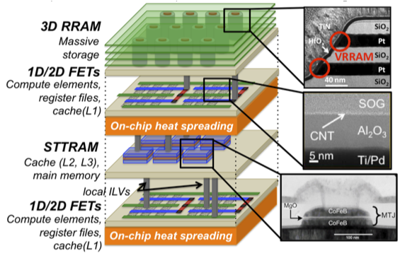
Figure 1. Monolithic 3D computing system: emerging logic and memory technologies, and on-chip thermal solutions. Circuits on various layers are vertically connected using high-density ILVs
Figure 1 shows a monolithic 3D computing system that can potentially achieve significant energy efficiency benefits compared to conventional architectures. Logic layers are fabricated using carbon nanotube FETs (1D FETs) or layered transition metal dichalcogenides (2D FETs). (The bottom-most layer can be implemented using silicon FETs). It also combines non-volatile memory technologies (STTRAM, 3D RRAM) and integrated thermal solutions. The various layers can be interleaved in a flexible fashion, enabled by low-temperature monolithic 3D fabrication. It can additionally tightly couple sensors with computing, enabling local processing of sensor data. Such monolithic 3D integration requires a deep understanding of and solutions to challenges related to variability, yield, and reliability.
Recent advances in carbon nanotubes (high-performance carbon nanotube FETs and system-level demonstration such as the carbon nanotube computer), STTRAM and RRAM, and their monolithic 3D integration enable this vision. These advances, however, can only be utilized to their full potential through a multidisciplinary framework from system architectures all the way to technology layers, together with demonstrations of meaningful experimental prototypes.
About the panel member:

Subhasish Mitra directs the Robust Systems Group in the Departments of Electrical Engineering and Computer Science of Stanford University, where he is the Chambers Faculty Scholar of Engineering. Before joining Stanford, he was a Principal Engineer at Intel.
Prof. Mitra’s research interests include robust system design, VLSI design, CAD, validation and test, emerging nanotechnologies, and emerging neuroscience applications. His X-Compact technique for test compression has been key to cost-effective manufacturing and high-quality testing of a vast majority of electronic systems, including numerous Intel products. X-Compact and its derivatives have been implemented in widely-used commercial Electronic Design Automation tools. His work on carbon nanotube imperfection-immune digital VLSI, jointly with his students and collaborators, resulted in the demonstration of the first carbon nanotube computer, and it was featured on the cover of NATURE. The National Science Foundation presented this work as a Research Highlight to the United States Congress, and it also was highlighted as "an important, scientific breakthrough" by the BBC, Economist, EE Times, IEEE Spectrum, MIT Technology Review, National Public Radio, New York Times, Scientific American, Time, Wall Street Journal, Washington Post, and numerous organizations worldwide.
Prof. Mitra's major honors include the Presidential Early Career Award for Scientists and Engineers from the White House, ACM SIGDA/IEEE CEDA A. Richard Newton Technical Impact Award in Electronic Design Automation, and the Intel Achievement Award, Intel’s highest corporate honor. He and his students published several award-winning papers at major venues: IEEE/ACM Design Automation Conference, IEEE International Solid-State Circuits Conference, IEEE International Test Conference, IEEE Transactions on CAD, IEEE VLSI Test Symposium, Intel Design and Test Technology Conference, and the Symposium on VLSI Technology. At Stanford, he has been honored several times by graduating seniors “for being important to them during their time at Stanford.” Prof. Mitra served on DARPA’s Information Science and Technology Board as an invited member. He is a Fellow of the ACM and the IEEE.
Secondary navigation
- EPFL Workshop on Logic Synthesis and Emerging Technologies
- Luca Amaru
- Luca Benini
- Giovanni De Micheli
- Srini Devadas
- Antun Domic
- Rolf Drechsler
- Pierre-Emmanuel Gaillardon
- Jie-Hong Roland Jiang
- Akash Kumar
- Shahar Kvatinsky
- Yusuf Leblebici
- Shin-ichi Minato
- Alan Mishchenko
- Vijaykrishnan Narayanan
- Ian O'Connor
- Andre Inacio Reis
- Martin Roetteler
- Julien Ryckaert
- Mathias Soeken
- Christof Teuscher
- Zhiru Zhang
- Symposium on Emerging Trends in Computing
- Layout synthesis: A golden DA topic
- EPFL Workshop on Logic Synthesis & Verification
- Luca Amaru
- Luca Benini
- Robert Brayton
- Maciej Ciesielski
- Valentina Ciriani
- Jovanka Ciric-Vujkovic
- Jason Cong
- Jordi Cortadella
- Giovanni De Micheli
- Antun Domic
- Rolf Drechsler
- Henri Fraisse
- Paolo Ienne
- Viktor Kuncak
- Enrico Macii
- Igor Markov
- Steven M. Nowick
- Tsutomu Sasao
- Alena Simalatsar
- Leon Stok
- Dirk Stroobandt
- Tiziano Villa
- Symposium on Emerging Trends in Electronics
- Raul Camposano
- Anantha Chandrakasan
- Jo De Boeck
- Gerhard Fettweis
- Steve Furber
- Philippe Magarshack
- Takayasu Sakurai
- Alberto Sangiovanni-Vincentelli
- Ken Shepard
- VENUE
- Panel on Circuits in Emerging Nanotechnologies
- Panel on Emerging Methods of Computing
- Panel on The Role of Universities in the Emerging ICT World
- Panel on Design Challenges Ahead
- Panel on Alternative Use of Silicon
- Nano-Bio Technologies for Lab-on-Chip
- Functionality-Enhanced Devices Workshop
- More Moore: Designing Ultra-Complex System-on-Chips
- Design Technologies for a New Era
- Nanotechnology for Health
- Secure Systems Design
- Surface Treatments and Biochip Sensors
- Security/Privacy of IMDs
- Nanosystem Design and Variability
- Past Events Archive