Go to
March 15, 2006
Next Generation Image Sensor
Toshihisa Watabe, Principal Research Engineer, NHK Science and Technical Research Laboratories, Tokyo, Japan
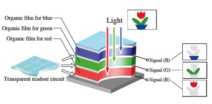
Abstract: In current professional-use cameras, such as broadcast television (TV) cameras, incident light through a lens is separated into three primary color components (blue, green and red) by a dichroic prism, and each color is then detected individually by one of three imaging devices, such as CCD. As the number of the pixel of the sensor is increasing to achieve a high-resolution, sensitivity is reduced due to shrinking the pixel area of the sensor. This low sensitivity is compensated by amplifying the signal output electrically especially when the camera is used to shoot pictures under low light conditions, so the picture quality (Signal-to-noise ratio) is degraded. Moreover, the dichroic prism makes a size of the camera large, so that the feature of handiness is reduced. To solve these problems, we have been researching a super-high sensitivity imaging devices with HARP (High-gain Avalanche Rushing amorphous Photoconductor) and a new type of solid-state image sensor overlaid with three kinds of organic photoconductive films which are sensitive to only blue, green, and red light to achieve compact, lightweight and high-resolution color camera without dichroic prism. These technologies also improve the potential of the imaging devices used in consumer products, such as digital cameras and cell phones, that is, improve the low sensitivity due to the decreasing pixel size which reaches 2 microns, and reduction of picture quality due to single sensor with mosaic color filters installed in the cameras. We discuss the developing techniques and issues for a next generation image sensor based on a new concept to achieve the highest sensitivity and picture quality.
About the speaker: Toshihisa Watabe received his B.E. and M.E. degrees in electronic engineering from Keio University, Yokohama, Japan, in 1989 and 1991, respectively. In 1991, he joined the Japan Broadcasting Corporation NHK, Tokyo, Japan. From 1991 to 1994, he worked at the Niigata regional broadcasting station of NHK as a television engineer. Since 1994, he has been engaged in the research and development of the highly sensitive CMOS image sensor, CMOS image sensor with organic photoconductive films, and highly sensitive field-emitter-array image sensor in the Advanced Boadcasting Devices Department of the NHK Science and Technical Research Laboratories where he currently is a principal research engineer.
Download visuals (3.3 MB pdf)
Secondary navigation
- January 29, 2018
- August 30, 2017
- Past seminars
- 2016 - 2017 Seminars
- 2015 - 2016 Seminars
- 2014 - 2015 Seminars
- 2013 - 2014 Seminars
- 2012 - 2013 Seminars
- 2011 - 2012 Seminars
- 2010 - 2011 Seminars
- 2009 - 2010 Seminars
- 2008 - 2009 Seminars
- 2007 - 2008 Seminars
- 2006 - 2007 Seminars
- August 31, 2007
- June 29, 2007
- June 20, 2007
- June 5, 2007
- May 30, 2007
- May 16, 2007
- May 15, 2007
- April 24, 2007
- March 27, 2007
- March 14, 2007
- February 9, 2007
- February 8, 2007
- January 12, 2007
- December 5, 2006
- November 14, 2006
- October 31, 2006
- October 27, 2006
- October 26, 2006
- October 20, 2006
- September 20, 2006
- September 20, 2006
- September 20, 2006
- September 19, 2006
- 2005 - 2006 Seminars
- August 23, 2006
- August 22, 2006
- June 26, 2006
- June 20, 2006
- June 16, 2006
- June 7, 2006
- June 6, 2006
- May 30, 2006
- May 17, 2006
- May 10, 2006
- April 27, 2006
- April 12, 2006
- March 31, 2006
- March 29, 2006
- March 22, 2006
- March 15, 2006
- February 27, 2006
- February 8, 2006
- January 25, 2006
- January 19, 2006
- January 18, 2006
- January 17, 2006
- January 11, 2006
- November 30, 2005
- November 23, 2005
- November 2, 2005
- October 26, 2005
- October 25, 2005
- October 5, 2005
- September 28, 2005
- 2005 Seminars
Links