Go to
February 22, 2008
Process aspect of increasing system level performance by 3D Integration
Deniz Sabuncuoglu Tezcan, IMEC (Interuniversity MicroElectronics Center), Leuven, Belgium
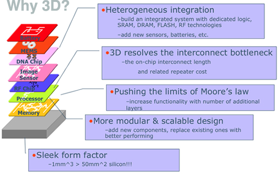
Abstract: Over the past 30 years and through scaling, the semiconductor industry has been able to continuously reduce the cost per function while simultaneously increasing the function density. However, technology roadblocks and the increased cost of ownership of scaled technology threaten to break this historic trend. Stacking of ICs and interconnecting them in the 3rd dimension, is an attractive alternative to 2D scaling that permits to continue system size reduction and to increase circuit performance while further reducing system cost. On the other hand, IC technology is specializing in different fields: microprocessors, memory, sensors, RF circuits and integration of these different technologies to make application specific systems becomes a challenge and 3D integration offers a solution. Many 3D integration schemes have been proposed in literature; and they can generally be classified according to the level at which the 3D interconnect breaks into the classical system interconnect hierarchy. Different technology platforms enable different 3D interconnect densities as well as a different electrical performance. Eventually, the different classes of 3D technologies will continue to co-exist since system requirements will dictate which technology options are viable for each specific application. Most of these 3D stacking "flavors" build on a combination of process technologies like wafer thinning, through wafer vias, dielectric isolation, conductive filling, bumping and flip-chip. The sequence and choice of the process technologies depend on the system level choices.
About the speaker: Deniz Sabuncuoglu Tezcan was born in Ankara, Turkey, in 1973. She received her B.S., M.S., and Ph.D. degrees in electrical engineering from Middle East Technical University (METU), Ankara, Turkey in 1995, 1997, and 2002, respectively. Her doctoral studies focused on uncooled infrared detectors implemented in CMOS technology. From 1995 to 2003, she was employed as a teaching/research assistant and later as an instructor in the Electrical and Electronics Engineering Department of METU. During her Ph.D., she was awarded with the Integrated Ph.D. Scholarship from the Scientific and Technical Research Council of Turkey (TUBITAK) to continue her studies partially at IMEC, Belgium and the Ph.D. Student Support Scholarship from ASELSAN Inc., Ankara, Turkey. In September 2003, she received the Post Doctoral Research Grant from Katholieke Universiteit Leuven, Belgium and continued her studies at IMEC. Since September 2005, she is employed by IMEC as Research Engineer specializing in process development and integration of various projects including 3D stacking of wafers/dies, through-wafer-vias for wafer level packaging, high performance active pixel CMOS imagers, Si:As blocked impurity band infrared detectors, wafer level liquid chromatographs and shock sensors. She is the author/co-author of more than 30 technical publications and has won the best paper award for "Development of Vertical and Tapered via Etch for 3D Through Wafer Interconnect Technology," at IEEE EPTC 2006.
Download visuals (8.9 MB pdf)
Secondary navigation
- January 29, 2018
- August 30, 2017
- Past seminars
- 2016 - 2017 Seminars
- 2015 - 2016 Seminars
- 2014 - 2015 Seminars
- 2013 - 2014 Seminars
- 2012 - 2013 Seminars
- 2011 - 2012 Seminars
- 2010 - 2011 Seminars
- 2009 - 2010 Seminars
- 2008 - 2009 Seminars
- 2007 - 2008 Seminars
- 2006 - 2007 Seminars
- August 31, 2007
- June 29, 2007
- June 20, 2007
- June 5, 2007
- May 30, 2007
- May 16, 2007
- May 15, 2007
- April 24, 2007
- March 27, 2007
- March 14, 2007
- February 9, 2007
- February 8, 2007
- January 12, 2007
- December 5, 2006
- November 14, 2006
- October 31, 2006
- October 27, 2006
- October 26, 2006
- October 20, 2006
- September 20, 2006
- September 20, 2006
- September 20, 2006
- September 19, 2006
- 2005 - 2006 Seminars
- August 23, 2006
- August 22, 2006
- June 26, 2006
- June 20, 2006
- June 16, 2006
- June 7, 2006
- June 6, 2006
- May 30, 2006
- May 17, 2006
- May 10, 2006
- April 27, 2006
- April 12, 2006
- March 31, 2006
- March 29, 2006
- March 22, 2006
- March 15, 2006
- February 27, 2006
- February 8, 2006
- January 25, 2006
- January 19, 2006
- January 18, 2006
- January 17, 2006
- January 11, 2006
- November 30, 2005
- November 23, 2005
- November 2, 2005
- October 26, 2005
- October 25, 2005
- October 5, 2005
- September 28, 2005
- 2005 Seminars
Links