
Go to
EPFL-CSEM Projects
Disclaimer
This page summarizes some joint projects between EPFL and CSEM. Of these, only some projects include EPFL researchers active in Centre SI.
We thank Massimo Monti for compiling this information.
 Improved BAW Resonators for RF Applications
C. Muller, M.-A. Dubois
Portable devices like cellular phones for example require the lowest possible power consumption. Significant efforts were made recently to improve the quality factor of the BAW resonators in order to satisfy the specifications in this application field. Q-factors above 800 were achieved.
Download project description file (114 KB pdf)
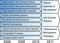 Microrobotics and packaging
Ulrich Claessen
The research partners of CSEM in the field of Microrobotics are ETHZ (Eidgenössische Technische Hochschule Zurich), EPFL (Ecole Polytechnique Fédérale de Lausanne), IMT(Institut de Microtechnique, Université de Neuchâtel), and HTA Luzern (Hochschule für Technik und Architektur).
Download project description file 2006 (60 KB pdf)
Download project description file 2007 (62 KB pdf)
 High-Precision Opto-Mechatronics for Astrophysics Instruments
L. Zago, P. Spanoudakis, J.-M. Mayor, S. Droz, L. Giriens, I. Kjelberg, P. Schwab, Y. Welte
Since 1997, CSEM has been developing and producing high-precision mechanisms for the latest generation of astronomical telescopes. These are high-precision opto-mechatronic systems combining fine sensing, control electronics and software to operate along multiple axes of motion. The typical accuracy of these systems is of the order of 0.1 μm and 1 μrad, respectively for linear and angular positions. CSEM provides the system engineering and integration support to a consortium including, among others, the Observatory of Geneva, EPFL and the Max Plank Institute for Astronomy. In 2006 the final design review was achieved and the DDL is now being fabricated for integration on site in late 2007.
Download project description file (151 KB pdf)
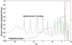 Photonic Crystal LEDs
R. P. Stanley, R. Houdré , N. Linder, M. Liley, H. Heinzelmann
A team comprising of EPFL, OSRAM Opto Semiconductor and CSEM set out to look at the possibilities of enhancing the directionality of LEDs by etching a photonic crystal in its surface.
Download project description file (32 KB pdf)
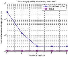 High Resolution Impulse Radio UWB Localization
J. Ayadi, H. Zhan, J. R. Farserotu
A new UWB ranging technique has been developed that outperforms the existing ones. A reduced-complexity version of this ranging technique can be flexibly implemented using FPGAs and hence it can be put on low-power silicon, which makes it a good candidate for high resolution localization and proximity ranging in wireless sensors based applications. An integration of the ranging technique in a UWB testbed being developed in the Swiss Federal Institute of Technology, Lausanne (EPFL), is under way.
Download project description file (21 KB pdf)
 Microfactory: A Flexible Assembly Platform
P. Glocker, R. Wyss, P. Schmid, U. Zbinden, J. Taprogge, M. Honegger, A. Steinecker, G. Gruener, C. Meyer
In the future, small components will be assembled on small machines. CSEM has designed small-sized Delta robots with integrated controller hardware and minimized external cabling and footprint. The PocketDelta is an ideal, modular, micro-assembly platform for automatic production in desktop applications. A demonstration Microfactory with four robots shows great potential for saving resources in miniaturized production systems.
Download project description file (77 KB pdf)
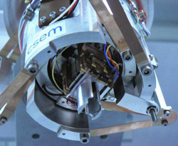
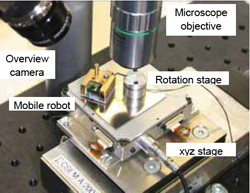 NanoHand - A System for Automated Nano-Handling - An Integrated EU Project
A. Steinecker
In the integrated EU-project NanoHand of FP6 a nano-manipulation platform will be developed that carries out automated nano-handling of nanotubes or nanowires. Individual handling of nano-components will be addressed inside or outside of a scanning electron microscope (SEM). It is targeted to build prototypes for design and testing of future nano-devices. Together with project partners CSEM realizes a system for nano-handling under a light microscope. Project partners: CSEM, EPFL, EMPA, Eurexcel (GB), Futuretech (DE), Klocke Nanotechnik (DE), Technical University Denmark - MIC (DK), Nascatec (DE), OFFIS (DE, Coordinator), ST Microelectronics (IT), VDI VDE-IT (DE).
Download project description file (4.8 MB pdf)
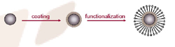 PAPAMOD
Development of novel methods for surface modification and investigation of cell-particles interaction for superparamagnetic nanoparticles.
Partners: LMIS-EPFL / CSEM, Alpnach / LTP-EPFL
Download project description file (551 KB pdf)
 Biochemical Nanofactory
René Paul Salathé, EPFL-STI-APL*, Jean-Marc Fournier, EPFL-STI-APL, Horst Vogel, EPFL-SB-LCPPM, Helmut Knapp, CSEM.
Downscale chemical's consumption and biotechnological production & analysis to the ultimate limits through Multiple optical tweezers for capturing arrays of particles, Micro-fluidics for addressing particles with reagents, and Fluorescence detection for analyzing time-resolved chemical reactions in parallel.
Download project description file (242 KB pdf)
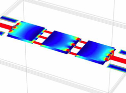
 Compact MEMS-based spectrometers for infra-red spectroscopy
M. Tormen, Ph. Niedermann, R. Lockhart, J-M. Mayor, R.P. Stanley
The design, fabrication and testing of deformable, diffractive MEMS gratings to be used as tuning elements in External Cavity Lasers (ECL) and MicroSpectrometers has been accomplished. The resulting devices are compact, fast, efficient and widely tuneable. The fabricated device consists of a free-standing, 1x1mm optical grating with an initial period of 12µm that can be stretched up to 3% by four sets of electrostatic comb drives. High optical efficiency of the diffractive device has also been achieved by blazing the elements using an anisotropic KOH etch.
Download project description file (1.3 MB pdf)
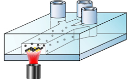
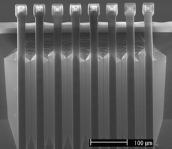 Hollow atomic force microscopy cantilevered probe arrays for nanoscale dispensing of liquids
J. Przybylska, A. Meister, Ph. Niedermann, M. Liley and H. Heinzelmann
This work reports on the top-down fabrication and the applications of new atomic force microscopy (AFM) probes dedicated to the on-demand dispensing of individual nanodroplets. The hollowness of the cantilever is used as a microfluidic channel that connects the reservoir located in the chip to the hollow tip. Focused ion beam (FIB) milling was used to open an aperture at the tip apex in order to permit the transfer of liquid towards the sample. The microfabrication of cantilevers with closed microfluidic channels relies on the fusion bonding and thermal oxidation of two pre-structured silicon wafers.
Download project description file (202 KB pdf)
 COMLAB
The global objective of Comlab is to supply a technology support for the R&D and production projects of CSEM, IMT (University of Neuchatel) and other publically funded R&D laboratories in the field of micro- and nanosystems like the CMI at the EPFL in Lausanne. In the future the collaboration between IMT and EPFL will be enforced.
Download project description file (54 KB pdf)
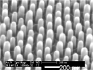 Tunable, high aspect ratio pillars on diverse substrates using copolymer micelle lithography: an interesting platform for applications
S. Krishnamoorthy, Y. Gerbig, C. Hibert, R. Pugin, C. Hinderling, J. Brugger and H. Heinzelmann
We demonstrate the use of copolymer micelle lithography using polystyrene-block-poly(2-vinylpyridine) reverse micelle thin films in their as-coated form to create nanopillars with tunable dimensions and spacing, on different substrates such as silicon, silicon oxide, silicon nitride and quartz. The promise of the approach as a versatile application oriented platform is highlighted by demonstrating its utility for creating super-hydrophobic surfaces, fabrication of nanoporous polymeric membranes, and controlling the areal density of physical vapor deposition derived titanium nitride nanostructures.
Download project description file (654 KB)
Other Collaborations
| 2007 | ||
| CMI Center of MicroNanotechnology | C. Hibert | Etching and nanofabrication |
| Integrated Systems Laboratory | G. De Micheli | Materials, Devices and Design Technologies for Nanoelectronic Systems Beyond Ultimately Scaled CMOS |
| Institute of Chemical Sciences and Engineering | H. Vogel | Fluorescent Nanoparticles |
| Microsystems Laboratory 2 | M. Gijs | Lab-on-a-chip for analysis and diagnostics |
| Laboratory for regenerative medicine and pharmacobiology | J. Hubbel | Generic scavenger powered DSPbased SoC for emerging implantable biosensors and bioactuators |
| Processor Architecture Laboratory | P. Ienne | Processor |
| Electronics Laboratory | M. Declercq | Medical processor 125 |
| Laboratory of Microengineering for Manufacturing | P. Ryser | Medical Processor |
| Microelectronic Systems Laboratory | Y. Leblebici | Materials, Devices and Design Technologies for Nanoelectronic Systems Beyond Ultimately Scaled CMOS |
| Microsystems Laboratory 1 | J. Brugger | Nanoscale structuring, nanofabrication |
| Nanostructuring Research Group | P. Hoffmann | Block copolymer self-assembly: Design of templated and chemically modified surfaces |
| Microsystems Laboratory 4 | P. Renaud | Superparamagnetic Nanoparticles |
| Ceramics Laboratory | P. Muralt | Sensors |
| Powder Technology Laboratory | H. Hofmann | Ceramics |
| 2006 | ||
| CMI Center of MicroNanotechnology | C. Hibert | Etching and nanofabrication |
| Institute of Chemical Sciences and Engineering | H. Vogel | Micro- and nanofabrication |
| Institute of Chemical Sciences and Engineering | H. Vogel | Fluorescent Nanoparticles |
| Institute of Quantum Electronics and Photonics | R. Houdré | Photonic crystal LEDs |
| Laboratory of Microengineering for Manufacturing | E. Meurville | Generic scavenger powered DSPbased SoC for emerging implantable biosensors and bioactuators (357 KB pdf) |
| Laboratory of Regenerative Medicine and Pharmacobiology | J. Hubbell | Polymer grafting, responsive polymeric layer |
| Laboratory of Nanostructures and Novel Electronic Materials | L. Forró | Carbon Nanotubes |
| Microsystems Laboratory 2 | M. Gijs | Lab-on-a-chip for analysis and diagnostics |
| Mobile Communications Laboratory | B. Rimoldi | Multi-user access for TOF cameras |
| Microsystems Laboratory 1 | J. Brugger | Nanoscale structuring, nanofabrication |
| Information Theory Laboratory | E. Teletar | Masters project on IR-UWB localization |
| Distributed Systems Laboratory | A. Schiper | Distributed systems over Wireless Sensor Networks |
PhD degrees Awarded by EPFL in 2006 to CSEM Collaborators
| Y. Keles | Synthesis of carbon nanotubes and characterization of nanotubes as atomic force microscopy tips |
| E. Gysels | Phase Synchronization for Classification of spontaneous EEG Signals in Brain-Computer Interfaces |
| S. Krishnamoorthy | Self-assembly of tunable, responsive polymer nanostructures: tools for nanofabrication of functional interfaces |
| I. Verettas | Microfabrique : méthodologie de conception de systèmes de production miniaturisés et modulaires, disposant d'un environnement salles blanches |
| J. Weingarten | Feature-based 3D SLAM |