
Go to
Gate-all-around Silicon Devices
Gate-all-Around Silicon Sub-Micron Devices and Integrated Photonics for On-Chip Signaling
Following Moore's law, the increasing reduction in the feature size of next generation's electronic technologies will provide smaller and faster devices, in larger number per unit of chip area, at lower cost per device. Electrical interconnects cannot keep pace with this evolution because the distance at which they can carry a signal without degradation is frequency limited. The reason is that the time constant of interconnection lines is invariant relative to size scaling and, as a consequence, with the rising of the working frequency, interconnects becomes limited at lower and lower distance while the demand is exactly the opposite due to the accompanying increase in the total chip area.
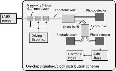
On-chip global clock distribution scheme based on silicon photonic wire waveguides and couplers, integrated SiGe based photodetectors and Gate All Around (GAA) light phase modulator. Co-integration with CMOS control logic is put in evidence.
Meanwhile, optical interconnects have already clearly been indicated as a very promising long time viable and reliable solution for board to board and chip to chip interconnections, while for on-chip interconnects a definitive vision has not yet been demonstrated.
Recently new extensive work has been performed to compare optical and electrical interconnects in terms of delay and power dissipation. Whereas, electrical interconnect performs better for local clock distribution and signaling interconnections of several μm's to 1 cm of length, optical interconnects become advantageous when distribution length exceeds a certain critical length.
Furthermore, the optical approach has other advantages such as immunity to electromagnetic interference, reduction of layer numbers, architecture simplification and unlike electronics optical circuits do not require design reconsideration when moving to next generations' technologies.
Low-loss (down to 0.8 dB/cm) optical waveguides with small bend radii have already been fabricated on a SOI platform. This allows for extremely compact silicon photonic devices.
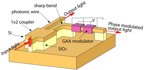
Possible implementation of the GAA modulator (in capacitive biasing configuration) in a SOI wafer. The GAA is fabricated by selective etching of the silicon dioxide in the region where the poly-silicon wrapping will be deposited.
Research Goals
The ITRS 2003 (International Technology Roadmap for Semiconductors) established three critical challenges for the future of optical interconnect.
- A high efficiency, high switching rate laser source, monolithically integratable into Si CMOS.
- A low power modulator, monolithically integratable into Si CMOS, to be used in conjunction with an off-chip continuous laser.
- Low power, high efficiency, small size optical detectors monolithically integratable into Si CMOS.
In this project we plan to address the last two issues, with the long-trem goal being a fully integrated guided-wave optical on-chip signaling system, based on advanced CMOS technology, and using an external light source.
For this purpose different research activities need to be undertaken:
- The development of low loss submicron optical wave guides (photonic wires), with active functionality through resonant structures.
- The development of a light phase modulator based on a Gate-All-Around MOS capacitor, offering at the same time high speed and low power consumption.
- The development of a CMOS compatible, small size and low power, optical photodetector for the IR spectral region.
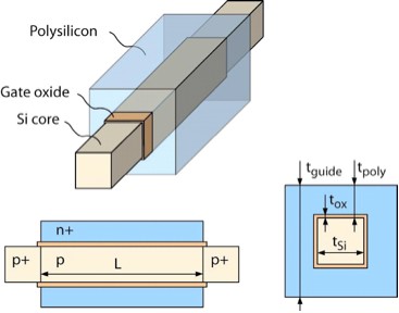
Conceptual view of a novel gate-all-around MOS device
Research Collaborators
Project leader: Adrian Ionescu
Electronics Laboratory, EPFL-STI-IMM-LEG
adrian.ionescu@epfl.ch
Project partner: Thomas Skotnicki
Advanced Devices Program Manager
STMicroelectronics, Crolles, France
thomas.skotnicki@st.com
Collaborator: Dr. Luc Thévenaz
Nanophotonics and Metrology Laboratory, EPFL-STI-ITOP-NAM
luc.thevenaz@epfl.ch
Participants: Paolo Dainesi (NAM + LEG2)
Kirsten Moselund (LEG)
ST Microelectronics, Crolles: Ph. Coronel, M. Bopp