Go to
Research
PRO3D: Programming for Future 3D Architecture with Many Cores
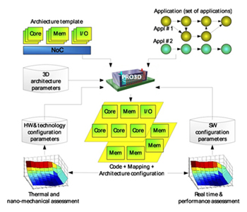 The shift from systems-on-chip (SoC) to manycore architectures brings new hardware and software challenges ranging from seamless integration of processors, memories, the design of modular systems and application software to run on massively parallel and scalable platforms. Manycores will benefit tremendously from 3-dimensional (3D) integration technology that enables distribution in space of computational and storage functions to achieve unprecedented performance levels.
PRO3D is an ambitious high risk and high reward project that builds upon existing European world-class R&D expertise of the partners. PRO3D will innovate in both hardware and software technologies and demonstrate the effectiveness of manycores by an integrated and concerted effort in key aspects of hardware and software design. The uniqueness of this proposal stems from the experience of the partners in various aspects of manycore design that need to be addressed concurrently.
The key outcome of PRO3D will be a holistic system design methodology to bring a drastic improvement of productivity to reduce cost development and time to market for future embedded computing. In particular, PRO3D will: i) develop a system software flow that can operate transparently on parallel manycore platforms; ii) develop formal methods for software design guaranteeing the composability and correct operation of both hardware and software; iii) explore the impact of 3D integration for new computing architectures iv) Extend the software-flow to 3D-stacked manycores.
The PRO3D consortium brings together world-class leaders in their own field with competencies to cover software, architecture and 3D integration. One of the key differentiators of the PRO3D consortium is its access to an industrial manycore System on Chip, named "Platform 2012" and provided by STM. The industrial impact of PRO3D is potentially high since research outcomes will be directly exploitatable into STM product roadmaps.
CMOSAIC: 3D Stacked Architectures with Interlayer Cooling
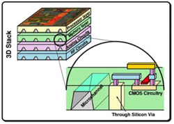 The CMOSAIC project is a genuine opportunity to contribute to the realization of arguably the most complicated system that mankind has ever assembled: a 3D stack of computer chips with a functionality per unit volume that nearly parallels the functional density of a human brain. CMOSAIC's aggressive goal is to provide the necessarily 3D integrated cooling system that is the key to compressing almost 1012 nanometer sized functional units (1 Tera) into one cubic centimeter with a 10 to 100 fold higher connectivity than otherwise possible. Even the most advanced air-cooling methods are inadequate for high performance 3D-IC systems where the main challenge is to remove the heat produced by multiple stacked dies in a 1-3 cm3 volume, each layer dissipating 100-150 W/cm2. State-of-the-art single phase liquid and two- phase cooling systems, using specifically designed microchannel arrangements, and employing coolants ranging from liquid water and two-phase environmentally friendly refrigerants to novel engineered nano-fluids offer significant advantages in addressing heat removal challenges leading to practical 3D systems. CMOSAIC aims at developing the engineering science base that will enable a new state of the art in high density electronics cooling.
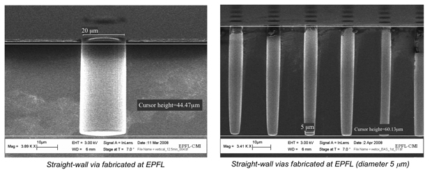
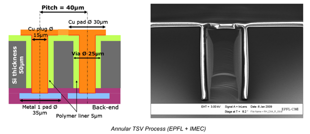
3D integration technologies at EPFL
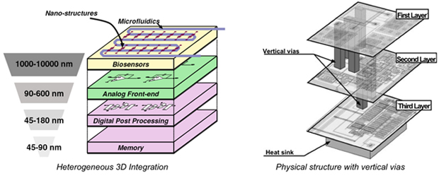
3D integration technologies are being developed at the EPFL Micro-Nano-Technologies Centre (CMI), in collaboration with IMEC, Microelectronic Systems Laboratory (LSM) and the Integrated Systems Laboratory (LSI). The targeted technology is based on chip-level post-processing of fabricated dies, using a via-last process, and it is intended to support homogeneous as well as heterogeneous 3D integration of multiple layers. The process relies on substrate thinning down to a thickness of 50 um, followed by annular via opening with a via hole diameter of 20 um, polymer filling of the trench, removal of the silicon core by DRIE technique, and subsequent copper electroplating of the via opening. This process was adopted from the already proven annular-etch TSV technology originally developed at IMEC, and was implemented in the CMI facility of EPFL, in 2009. The developed TSV and 3D integration technologies are expected to allow experimental realization of heterogeneous 3D stacks consisting of various species of chips, including bio-sensor layers combined with analog read-out and amplification, as well as digital processing and memory layers for complex data elaboration.