
Go to
Cell-Electronics Interface
Advanced Cell - Electronics Interface for Implanted Devices and Brain - Machine Interaction
Overview:
Interfaces between living matter and electronics are rapidly becoming a main topic of interest in neurosciences, especially in the search of efficient tools to monitor the electrical activity of living cells. The knowledge extracted from in-vitro measurements allows building a deeper understanding of the electrical behavior of cell clusters, leading to the derivation of more accurate models of larger parts of mammalian central nervous system. Such research activities are usually conducted with the end-goal of understanding how information is processed, stored and retrieved in the neocortex circuitry.
Spatio-temporal monitoring of the electrical activity of a cell culture, as well as electrical stimulation of a limited number of sites are the two main operations demanding complex external systems to support the experiments. Combined expertise in the domains of sensor interfaces, microelectronics, data acquisition and processing are needed to design and implement the tools for neuroscience experiments. Standards methods and tools applied in research include patch-clamping of single electrodes and micro-electrode arrays. Recently, silicon micro-machining techniques have been applied for the fabrication of arrays of electrodes. The first system for in-vivo capture of voluntary cortical signals to be interpreted as cursor movements with human cortical implantation has been reported in 2006. However, the majority of such electrode arrays have a spatial resolution of tens or hundreds of micrometers, i.e., the same order of magnitude as (or larger than) the dimension of typical neuron cells. In order to extract detailed information about the operation of and communication between individual neuron cells, the density of electrode arrays will have to improved by at least one order of magnitude - reaching a spatial resolution of micrometers. In addition, the electrode array system must eventually allow simultaneous monitoring as well as stimulation of the nerve cell tissue that is placed (grown) on the surface.
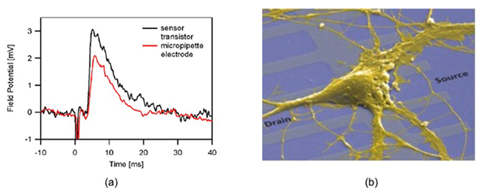
Figure 1. (a) State-of-the-art: monitoring of cell membrane potential of a firing neuron using sensor transistors (after Fromherz) (b) State-of-the-art: example of a neuron cell placed on a transistor array for monitoring (after Fromherz).
Research goals:
A number of key challenges will have to be addressed for the successful demonstration of a dense neuro-electrode array on chip. The study of the electrical behavior of clusters of cells has to be conducted in a way that supports stringent experimental constraints due to the very specific nature of the operation of living tissues. Environmental constraints are related to the cell culture forming an aggressive microenvironment for silicon-based devices, as well as its specific conductive property which acts adversely to the requirement of localized electrical stimulation. Moreover, the envisioned system requires the development of original packaging technologies. Electrical constraints associated with cell physiology dictate a limit to the local stimulation electric field. At the same time, the readout signals are heavily influenced by 1/f noise.
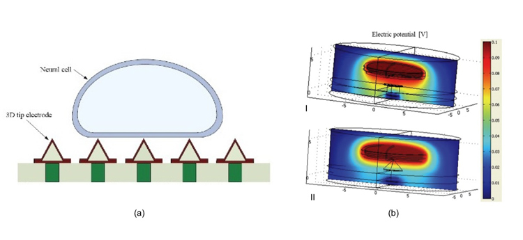
Figure 2. (a) Cross-section of a neural cell lying on the tips of a three-dimensional tip electrode array. (b) Electric potential simulation of a 10 um diameter neural cell with an intracellular potential equal to 100 mV lying on top of I. a 4 um diameter planar electrode and II. a 2.2 um diameter three-dimensional tip electrode.
The goal is to design, fabricate and experimentally demonstrate a dense 2-D (or 3-D) array of electrodes which can be integrated with deep submicron CMOS electronic circuitry directly underneath. The electrode array will first be demonstrated as a stand-alone structure, and subsequently developed as a post-processing step that can be added to a fabricated CMOS substrate. Every electrode in this very dense array should be addressable in read/write mode, whereas only some of electrodes are selected for actual processing at any given moment, depending on the actual position of the cells. The parallel goal is to develop the required sensing and stimulation circuitry in deep submicron CMOS technology, which will be essential for "closing the loop". These two efforts will be merged into the realization of a monolithic and very high-resolution multi-electrode array on-a-chip. Measurements must include standard electrical characterization, as well as in-vitro measurements.
Research Collaboration:
This research project will be carried out by the Microelectronic Systems Laboratory of Professor Yusuf Leblebici. The fabrication of the proposed micro-electrode array will be undertaken in the CMI facility of EPFL, which offers unique expertise and fabrication possibilities for the choice of materials and device geometries. In-vitro experiments will be conducted in close collaboration with researchers of the Brain and Mind Institute, and in particular, with the Neural Microcircuitry Laboratory of Professor Henry Markram.