
Go to
Building 3-D Architectures
Overview
The current trend in embedded consumer electronics has been increased complexity of new communications and multimedia standards. Ever-increasing processing requirements and strict time-to-market constraints eliminate the possibility of designing the vast majority of embedded systems from scratch. At present, embedded computing solutions range from fine-grained reconfigurable architectures-namely Field Programmable Gate Arrays (FPGAs) - on the one hand, to heterogeneous Multi-Processor Systems-on-Chips (MPSoCs) on the other. MPSoCs comprise a multitude of processors, Application-Specific Integrated Circuits (ASICs), and reconfigurable logic, along with a Network-on-Chip (NoC) that connects the various processing elements. MPSoC solutions for modern embedded architectures include platforms developed by major semiconductor vendors such as Philips Nexperia, TI OMap, and ST Nomadik.
Recent advancements in the creation of vertical interconnects enables the development of 3D tiered architectures. The greatest economic advantage of a 3D tiered architecture is greater yield. It is well known that smaller chips have a higher yield, or alternatively, a lower defect rate when fabricated. Consequently, a higher yield can be achieved by partitioning a circuit into k smaller sub-circuits, each of which will be fabricated and stacked, than building a single larger chip that contains all of the sub-circuits on the same die. Even if the performance of a 3D stacked architecture cannot compete with an equivalent 2D single chip design, the overall gain in yield could still easily justify the efficacy of the 3D layering approach.
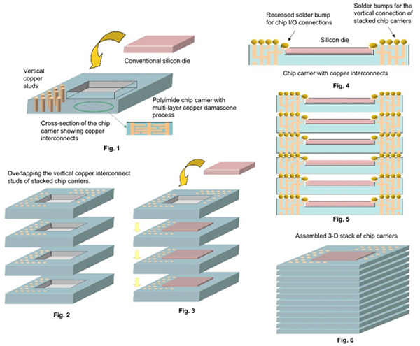
"Chip carriers" hold the conventional silicon dies and provide necessary vertical electrical contacts to the lower and higher strata. The chip carrier itself consists of a passive substrate, with multi-tier metallization and vertical studs to enable routing of signals. Figs. 1-3: Chip carriers illustrated. Fig. 4: Solder bumps also serve the purpose of mechanically holding the assembled die in place. Fig. 5: Cross-section of an assembled stack with solder bumps linking the strata together. Fig.6: The conceptual view of an assembled stack of chip carriers.
Research collaboration
- Processor Architecture Laboratory (LAP - Prof. Paolo Ienne)
- Microelectronic Systems Laboratory (LSM - Prof. Yusuf Leblebici)
- Integrated Systems Laboratory (LSI - Prof. Giovanni DeMicheli)
This project intends to harness the collective knowledge and abilities of the three EPFL laboratories, LAP, LSM and LSI to develop design methodologies, circuit architectures and technological solutions for 3D integrated circuits. The project involves several different research axes. The three laboratories involved in the project will be conducting this research in close collaboration with each other. At the end of the project, a working prototype that will demonstrate different aspects of 3D integrated circuits will be developed.
The first axis, which is the lowest level, is driven primarily by the LSM. This axis focuses on technological challenges involved in the design of vertical interconnections. The intermediate axis, driven primarily by the LAP, focuses on the processing and communication mechanisms used by a 3D tiered architecture, along with the necessary software support for compilation and synthesis. The highest level, driven by the LSI, focuses on modeling with specific emphasis on thermal emulation, resource allocation, and planning. These three axes are strongly linked to one another, and we believe that progress can be made on all three in parallel.
Research goals
In the end, this project will produce a demonstrator to show that the overall idea of 3D tiered architectures is feasible. The demonstrator will be relatively simple -most likely, only a few tiers with modest vertical interconnection resources, but will be sufficient to show initial results of the more forward-looking research on thermal issues of the LSI and LAP.