
Go to
Fault-Tolerant Design
Fault-Tolerant Design of Memory Arrays and PLAs With Failure-Prone Nanometer-Scale Technologies
Overview:
Emerging nanometer-scale device technologies such as carbon nanotubes, polysilicon nanowires, and single electron transistors hold the promise of dramatically increased integration densities for future nanosystems, coupled with significantly reduced power dissipation. While silicon-based solutions are generally preferred in order to simplify the interfacing of such devices with existing electronics, the integration of non-silicon nanodevices with silicon interfaces is also explored. However, both silicon-based and non-silicon based nanodevices are expected to suffer from dramatically increased transient and permanent failure rates, mainly due to the quantum nature (hence, to the probabilistic behavior) of the devices, and also due to the fundamental limitations of the fabrication processes that limit the yield of such devices.
Thus, the necessity to cope with intrinsic errors at the device and circuit level must be recognized as a key aspect of nano-scale systems design. To implement such robustness and fault tolerance, new circuit design approaches will need to be considered. At the same time, the path to high-level (top-down) synthesis should ideally remain compatible with the established design approaches. A likely future scenario is that the functional blocks be designed with a certain degree of fine-grained, built-in immunity to such permanent and transient faults, such that they are capable of absorbing a number of errors and still be able to perform their functions. This type of pervasive fault tolerance, which is based on the implicit acceptance that a certain percentage of devices in the system will fail in a random fashion, may require a novel approach to robust design that is quite different from classical techniques of fault-tolerance and redundancy.
Currently, the strategy for system design is based on the hierarchical characterization of several levels of abstraction, from device to architectural high level, with intrinsic verification methods and tools for each level. With highly unreliable components, such as the ones expected in the nanotechnology era, the design methodologies will have to take into account the reliability as a substantial factor, allowing the design of reliable systems from unreliable components.
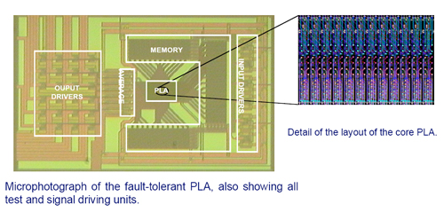
The specific goal of this project is to explore the design of inherently reliable PLA structures and memory arrays that can eventually be used as essential building blocks of complex nano-electronic systems.
Research Goals:
Our approach is to particularly develop and apply fault and defect tolerance techniques at various levels of complexity but dealing with a technology dependent reality. Based on these results, we will then consider the possibility of very high abstraction and evaluate a technology independent defect tolerant architecture. The technologies that will be in the modelling and fabrication focus at nano-scale are:
- Silicon nano-CMOS, which will serve as fast platform of validation of advanced concepts of defect tolerance,
- Single (or Tunneling) Electronics and CMOS/SET (or tunneling) hybrids, as first alternative technology dealing with power density and speed trade-off together with new possible functionalities. The obtained results could be extended furthermore to a much more general class of tunneling devices.
- Carbon nanotubes and CMOS/CNTs hybrids, as second alternative technology dealing with very dense nano-systems in which CNT could also play a major role for horizontal and vertical interconnects.
Research Collaborators:
This research project will be conducted in close collaboration among the following three research groups:
- Microelectronic Systems Laboratory (LSM - Prof. Yusuf Leblebici)
- Integrated Systems Laboratory (LSI - Prof. Giovanni DeMicheli)
- Electronics Laboratory (LEG - Prof. Adrian Ionescu)
As such, the research will span a fairly wide spectrum, ranging from device physics and nanoelectronic device fabrication to circuit design and optimization, and to system design and design automation.