Since the introduction of the Metal-Oxide-Semiconductor Field Effect Transistor (MOS-FET), the semiconductor industry has been able to reduce the dimensions of the transistors at a regular pace, as captured by Moore’s Law. Devices with feature sizes below 20nm have been fabricated using new materials and processing steps. A recent important innovation is the introduction of non-planar geometries with fins and tri-gate structures. Following this trend, Silicon NanoWires (NW) coupled to Gate-All-Around (GAA) structures appear as a promising solution to further reduce the dimensions of the transistors and to improve electrostatic control.
Device downscaling has correlated with increased performances of integrated circuits and systems, as well as increased functionality per unit area. As downscaling becomes increasingly more expensive in terms of fabrication facility costs, we propose an alternative path to Moore’s Law where, instead of downscaling the dimensions of the transistors any further, we focus on increasing their functionality for a given area.
Multiple-Independent-Gate (MIG) FETs, a novel class of devices that demonstrates enhanced functionality and flexibility as compared to standard MOSFETs. MIGFETs are GAA Schottky-Barrier (SB) NWFETs with multiple gate regions that control independently the properties of the semiconductor channel. For practical reasons, we focus on a device with three independent gate regions called Three-Independent-Gate (TIG) FET. In addition to a conventional gate, the device has two gated regions over the SB. Independently controlling the SB at the source and drain of the device allows us to modulate the barrier heights and therefore to select the carrier type to inject into the device. The modulation of the SB enables a dynamic control of both the polarity and the threshold of the device at runtime. Having a device with different modes of conduction that can be changed at runtime leads to many circuit-level opportunities. In particular, a dynamic control of the device polarity enables the realization of compact binate operators, such as a 4-transistor XOR operator. Similarly, it is possible to create compact unate combinational logic gates, such as NAND or MAJ gates, as well as compact memory primitives, such as a compact True-Single Phase Clock (TSPC) flip-flop or 4-transistor Static Random Access Memory (SRAM). Moreover, this device can be used fruitfully within low-power circuit design. Its multiple-VT control allows designers to realize high-VT or low-VT logic gates with a unique type of transistor, while power-gating architectures can be realized with no additional sleep transistors. In order to demonstrate the capabilities of the presented technology, we consider an application case study, where different design approaches are used to implement a telecommunication circuit. The realization of a polar code decoder with a 22-nm TIGFET technology leads to 20% faster and 32% more energy efficient system compared to its FinFET counterpart, at a moderate area overhead of 15%.
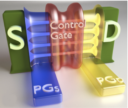
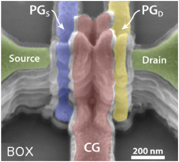
Left: Conceptual sketch of a TIG SiNWFET Right: SEM image of the fabricated TIG SiNWFET
A conceptual sketch of the TIG SiNWFET is given above left. Four vertically-stacked nanowires are confined within the source and drain pillars. They are surrounded by three independent gate structures, named Polarity Gate at Source (PGS), Control Gate (CG) and Polarity Gate at Drain (PGD). Metallic source and drain form Schottky junctions with the silicon channel. Image above right shows the SEM image of the final device.
Resistive Random Access Memories (ReRAMs) are one of the most promising candidates to replace flash memories due to fast access speed, low voltage operation, simple structure and compatibility with current CMOS technology. Besides stand-alone memories, ReRAMs are a fundamental building block for applications such as neuromorphic circuits and future generation FPGAs. In this research, we develop novel memory stacks suited to reconfigurable logic and work on a heterogeneous integration of ReRAMs with standard CMOS technology by post-processing the Back-End-of-the-Line (BEOL) of fully finished CMOS chips.
The ReRAM device functionality is based on a solid-state redox process induced by oxygen migration creating conductive filamentary paths in an insulator material. The reversibility of this process allows a hysteretic resistance that can be used as memory element, switching between a High Resistance State (HRS) and a Low Resistance State (LRS). Many parameters influences the stack performances such as the geometries, the materials and the deposition techniques. In the list of possible transition-metal oxides for ReRAMs, TaOx has been selected as switching material for its outstanding retention and endurance characteristics.
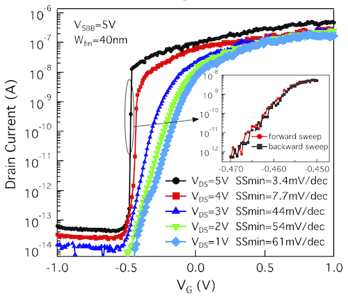
In low-power applications, small operation voltages and leakage currents are considered as the main technology means to reduce power consumption. However, the fundamental limitation of Subthreshold Slope (SS) in conventional MOSFETs (~60 mV/dec at room temperature) becomes the bottleneck for continuously lowering the operation voltages. To break this limit, different types of devices have been proposed based on various mechanisms, each with its own drawbacks. Our device, a steep SS silicon FinFET with Schottky-barrier source/drain, shows a minimal SS of 3.4 mV/dec and an average SS of 6.0 mV/dec over 5 decades of current swing. Ultra-low leakage floor of 0.06 pA/μm is also achieved with high Ion/Ioff ratio of 107.

The fin-based device structure is shown in the figure given on the right. The Schottky-Barrier Bias (SBB) electrostatically modulates the Schottky barriers at S/D, while the gate controls the potential barrier in the channel to turn the device on or off. Violet: Schottky-Barrier Bias (SBB) region modulating the Schottky barriers. Red: Gate controlling the channel conduction.
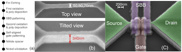
Fabrication of the proposed device: (a) Process flow. (b) SEM image of the fin, Hfin=340 nm, Wfin after fin etching are 50 nm, 60 nm and 70 nm. (c) SEM image of the final device, Lgate=200 nm, Tox ~15 nm. Total channel length ~600 nm, the final Wfin are 40 nm, 50 nm and 60 nm considering the silicon consumed during oxidation.
Working principle
For n-type behavior, i.e., when VSBB>0, electrons are selected to tunnel through the Schottky barrier into the channel. When VG is at threshold voltage, a transition occurs in the device. Weak impact ionization generates electron/hole pairs. The generated electrons drift to the drain, and the holes accumulate in the potential well induced by the gate. This lowers the barrier, and provides more electrons for impact ionization. Then, more accumulated holes continue to lower the barrier and thus form a positive feedback. In addition to the FinFET structure enhancing carrier multiplication, the second important contribution is from the dynamic modulation of the Schottky barrier. Parts of the generated holes are swept towards the source, increasing the hole density in SBB region. This helps to lower the energy band under SBB. Schottky barrier at source becomes thinner and more electrons tunnel through it. In the meantime, the potential well is kept until the final on state. This mechanism improves the Ion/Ioff ratio, and is considered as a key to achieve steep transition for 5 decades of current. The operation of p-type is similar but with VSBB<0.
2-dimensional graphene-like monolayers and few-layers semiconducting transition metal dichalcogenides (TMDCs) have recently drawn considerable attention as viable candidates for flexible and beyond-CMOS electronics and have shown the potential for the realization of polarity controllable devices. The most studied material among TMDCs, molybdenum disulphide (MoS2), suffers from Fermi level pinning to the conduction band at the metal-semiconductor interface which makes it challenging to achieve an ambipolar behavior, necessary for the realization of polarity-controllable devices. Thus, we focused on different 2D-TMDCs, such as tungsten diselenide (WSe2), that has shown the ability to efficiently conduct both type of charge carriers. We exploited the ambipolar behavior of WSe2 to realize double-independent back-gated devices and polarity-controllable behavior has been demonstrated with ON/OFF current ratios > 106 for both polarities, on the same device. The device was realized on multilayer WSe2 flake (7.5 nm thick), that was transferred and aligned on a substrate where buried metal lines were used as PG and the silicon substrate as CG (see Figure). The metal contacts were realized using evaporated Titanium (Ti)/Palladium (Pd), which provide a band-alignment suitable for the injection of both charge carriers (near mid-gap contacts). The ambipolar behavior of the device can be seen in sub-Figure b, where the PG and CG gates where kept at the same potential during the voltage sweep. When using the two gates independently, the transistor polarity could be dynamically changed by the PG, while the CG controlled the ON/OFF status of the device (sub-Figures c,d). The experimental transfer characteristics measured showed a p-type behavior for VPG < 6V, sub-Figure c, while n-type conduction properties are shown for VPG > 4V, sub-Figure d, on the same device. The proposed approach of controlling the polarity of an undoped SB-FET through an additonal gate, is relatively simple to implement, as Schottky barriers are much easier to create than Ohmic contacts in low-dimensionality materials, and is adaptable to any 2D-semiconductor.
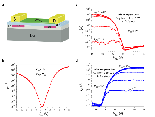
Polarity-control in 2D-WSe2 Double-Independent-Gate-FETs.(a) 3D-schematic view of the device. The silicon wafer acts as CG, while the PG have been patterned before the flake transfer. (b) experimental transfer characteristic of the device measured with the same bias applied to CG and PG. The gate leakage current is also plot. (c) p-type transfer characteristics obtained for multiple negative biases of the PG gate and sweeping the CG. The leakage currents of both gates are also plotted. (d) n-type transfer characteristics obtained for multiple positive biases of the PG gate and sweeping the CG. The leakage currents of both gates are also plotted.
Controlled polarity transistors in WSe2 have been used to design and realize a simple library comprising six basic cells for digital design.
Main Publications